- Courses
- Tutorials
- Interview Prep
GATE EC || ANALOG ELECTRONICS|| PYQs (2000-2025)
Question 1
For the circuit in the below figure, the voltage V0 is (ASSUME IDEAL DIODE)
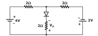
(GATE 2000 || EC || MCQ || 2 MARKS)
2V
1V
-1V
None of the above
Question 2
For the circuit shown in figure. D1 and D2 are identical diodes with utility factor of unity. The thermal voltage VT = 25 mV.
(a) Calculate V1 and V2.
(b) If the reverse saturation current of D1 and D2 are 1 pA then compute the current I through the circuit.
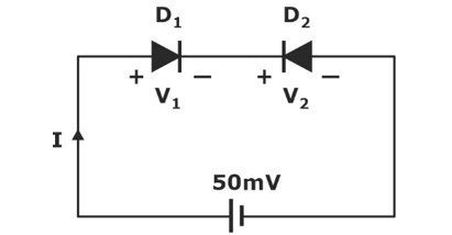
(GATE 2001 || EC || PYQ || NAT || 5 MARK)
V1 = 14.15 mV, V2 = 35.85 mV
I = 0.76pA
Question 3
The circuit shown in the figure is best described as a
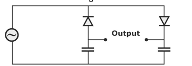
(GATE 2003 || EC || PYQ || MCQ || 1 MARK)
bridge rectifier
ring modulator
frequency discriminatory
Voltage doubler
Question 4
In a full-wave rectifier using two ideal diodes, Vdc and Vm are the dc and peak values of the voltage respectively across a resistive load. If PIV is the peak inverse voltage of the diode, then the appropriate relationships for this rectifier are
(GATE 2004 || EC || PYQ || MCQ || 2 MARK )
[Tex]V_{dc} = \frac{V_m}{\pi}, \quad \text{PIV} = 2V_m[/Tex]
[Tex]V_{dc} = \frac{2V_m}{\pi}, \quad \text{PIV} = 2V_m[/Tex]
[Tex]V_{dc} = \frac{2V_m}{\pi}, \quad \text{PIV} = V_m[/Tex]
[Tex]V_{dc} = \frac{V_m}{\pi}, \quad \text{PIV} = V_m[/Tex]
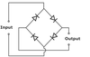
Question 5
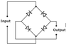
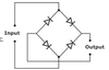
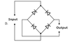
The correct full wave rectifier circuit is
(GATE 2007 || EC || PYQ || MCQ || 1 MARK)
Question 6
In the circuit below, the diode is ideal. The voltage V is given by
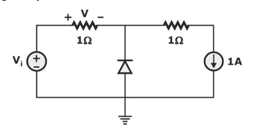
(GATE 2009 || EC || PYQ || MCQ || 2 MARK)
min (Vi, 1)
max (Vi, 1)
min (–Vi, 1)
max (–Vi, 1)
Question 7
In the circuit shown below, assume that the voltage drop across a forward bias diode is 0.7 V. The thermal voltage [Tex]V_t = \frac{KT}{q} = 25\ \text{mV}[/Tex]. The small signal input [Tex]V_i = V_p \cos(\omega t)[/Tex] where [Tex]V_p = 100\ \text{mV}[/Tex].

The bias current IDC through the diodes is
( GATE 2011 || EC || PYQ || MCQ || 2 MARK)
1 mA
1.28 mA
1.5 mA
2 mA
Question 8
In the circuit shown below, assume that the voltage drop across a forward bias diode is 0.7 V. The thermal voltage [Tex]V_t = \frac{KT}{q} = 25\ \text{mV}[/Tex]. The small signal input [Tex]V_i = V_p \cos(\omega t)[/Tex] where [Tex]V_p = 100\ \text{mV}[/Tex]. The ac output voltage Vac is
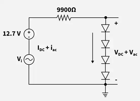
(GATE 2011 || EC || PYQ || MCQ || 2 MARK)
0.25 cos(ωt) mV
1 cos(ωt) mV
2 cos(ωt) mV
22 cos(ωt) mV
Question 9
The diode and capacitors in the circuit shown are ideal. The voltage v(t) across the diode D1 is
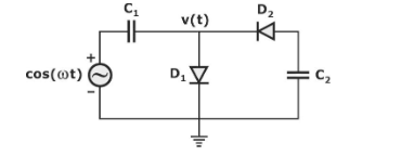
(GATE 2012 || EC || PYQ || MCQ || 1 MARK)
cos(ωt) – 1
sin(ωt)
1 - cos(ωt)
1 - sin(ωt)
Question 10
A voltage 1000sinωt volts is applied across YZ. Assuming ideal diodes, the voltage measured across WX in volts, is
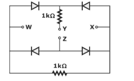
(GATE 2013 || EC || PYQ || MCQ || 2 MARK)
sinωt
[Tex]\frac{\sin \omega t + |\sin \omega t|}{2}[/Tex]
[Tex]\frac{\sin \omega t - |\sin \omega t|}{2}[/Tex]
0 for all t
There are 146 questions to complete.