- Courses
- Tutorials
- Interview Prep
GATE EC|| DIGITAL LOGIC || COMBINATIONAL CIRCUIT || PYQS(2000-2025)
Question 1
In a half-subtractor circuit with inputs X and Y, find the expressions for Borrow (M) and Difference (N = X − Y).
(GATE 2014 || EC || MCQ || 1 MARK )
M = X ⊕ Y, N = XY
M = XY, N = X ⊕ Y
M = X̄Y, N = X ⊕ Y
M = X Ȳ, N = (X ⊕ Y)̄
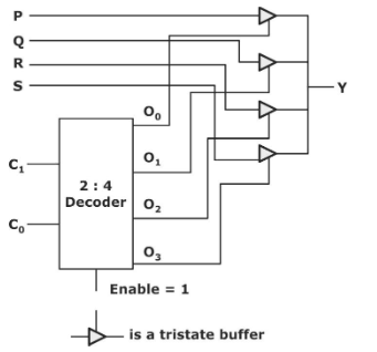
Question 2
In the circuit shown below, P and Q are the inputs. The logical function realized by the circuit shown below is
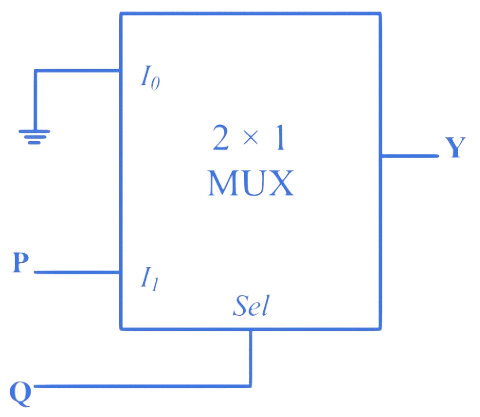
( GATE 2023 || EC || PYQ || NAT || 1 MARK)
Y = PQ
Y = P + Q
Y = (PQ)̄
Y = P̄ + Q̄
Question 3
Consider the circuit shown in the figure.
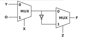
The Boolean expression F implemented by the circuit is
( GATE 2016 || EC || PYQ || MCQ || 1 MARK )
X̅Y̅Z̅ + XY + Y̅Z
X̅YZ̅ + XZ + Y̅Z
X̅Y̅Z̅ + XY + Y̅Z
X̅Y̅Z̅ + XZ + Y̅Z
Question 4
For the circuit shown in the figure, the delays of NOR gates, multiplexers and inverters are 2 ns, 1.5 ns and 1 ns, respectively. If all the inputs P, Q, R, S and T are applied at the same time instant, the maximum propagation delay (in ns) of the circuit is:
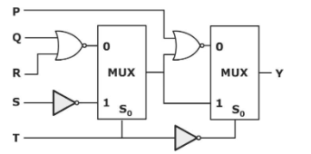
( GATE 2016 || EC || PYQ || MCQ || 1 MARK )
6
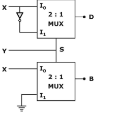
Question 5
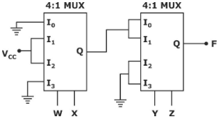
A 4: 1 multiplexer is to be used for generating the output carry of a full adder. A and B are the bits to be added, while Cin is the input carry and Cout is the output carry. A and B are used as the select bits, with A being the more significant select bit.
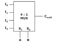
Which one of the following statements correctly describes the choice of signals to be connected to the inputs I0, I1, I2 and I3 so that the output is Cout?
( GATE 2014 || EC || PYQ || MCQ || 1 MARK )
I0 = 0, I1 = Cᵢₙ, I2 = Cᵢₙ, I3 = 1
I0 = 1, I1 = Cin, I2 = Cin, I3 = 1
I0 = Cin, I1 = 0, I2 = 1, I3 = Cin
I0 = 0, I1 = Cin, I2 = 1, I3 = Cin
Question 6
The functional implement by the circuit below is
( GATE 2016 || EC || PYQ || MCQ || 1 MARK )
2-to-1 multiplexer
4-to-1 multiplexer
7-to-1 multiplexer
6-to-1 multiplexer
Question 7
Identify the circuit below,
( GATE 2014 || EC || PYQ || MCQ || 1 MARK )
Binary to gray code converter.
Binary to XS3 converter.
Gray to binary converter.
XS3 to binary converter.
Question 8
A 16-bit ripple carry adder is realized using 16 identical full adders (FA), as shown in the figure. The carry-propagation delay of each FA is 12 ns, and the sum-propagation delay of each FA is 15 ns. The worst-case delay (in ns) of this 16-bit adder will be:
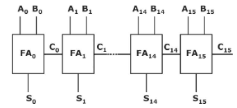
(GATE 2014 || EC || MCQ || 1 MARK)
(194.9 to 195.1)
Question 9
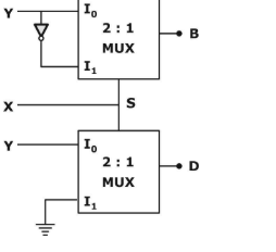
If X and Y are inputs and the Difference (D = X – Y) and the Borrow (B) are the outputs, which one of the following diagrams implements a half-subtractor?
(GATE 2014 || EC || PYQ || MCQ || 1 MARK)

Question 10
In the circuit shown, W and Y are MSBs of the control inputs. The output F is given by
( GATE 2014 || EC || PYQ || NAT || 1 MARK )
F = W X̄ + W̄ X + Ȳ Z
F = W X̄ + W̄ X + Ȳ Z̄
F = W X̄ Ȳ + W̄ X Ȳ
F = (W̄ + X̄) Ȳ Z
There are 21 questions to complete.