- Courses
- Tutorials
- Interview Prep
GATE EC || DIGITAL LOGIC || LOGIC FAMILY || PYQS (2000-2025)
Question 1
A standard CMOS inverter is designed with the equal rise and fall times (βn = βp). If the width of the PMOS transistor in the inverter is increased, what would be the effect on the LOW noise margin (NML) and the HIGH noise margin NMH?
(GATE 2019 || EC || MCQ || 1 MARK)
NML increases and NMH decrease
Both NML and NMH increase
No change in the noise margins
NML decreases, and NMH increases
Question 2
The full forms of the abbreviations TTL and CMOS in reference to logic families are
(GATE 2009 || EC || MCQ ||1 MARK)
Triple Transistor Logic and Chip Metal Oxide Semiconductor.
Tristate Transistor Logic and Chip Metal Oxide Semiconductor.Transistor-Transistor Logic and Complementary Metal Oxide Semiconductor.
Tristate Transistor Logic and Complementary Metal Oxide Silicon.
Question 3
The circuit diagram of a standard TTL NOT gate is shown in the figure. When Vi =2.5V, the modes of operation of the transistors will be
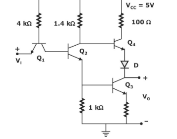
(GATE 2007 || EC || MCQ || 2 MARK)
Q₁: normal active;
Q₂: saturation;
Q₃: cut-off;
Q₄: cut-off
Q1: reverse active;
Q2: saturation;
Q3: saturation;
Q4: cut-off
Q1: normal active:
Q2: cut-off;
Q3: cut-off;
Q4: saturation
Q1: saturation;
Q2: saturation;
Q3: saturation;
Q4: normal active
Question 4
The transistors used in a portion of the TTL gate shown in the figure have a β = 100. The base-emitter voltage is 0.7 V for a transistor in the active region and 0.75 V for a transistor in saturation. If the sink current I = 1 mA and the output is at logic 0, then the Current IR will be equal to
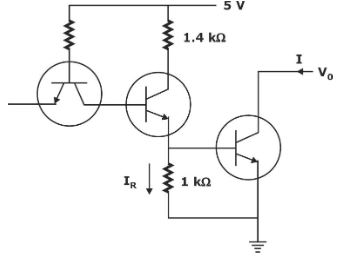
(GATE 2005 || EC || MCQ || 1 MARK)
65 mA
70 mA
0.75 mA
1.00 mA
Question 5
Given figure is the voltage transfer characteristic of
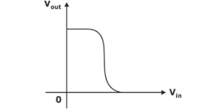
(GATE 2004 || EC || MCQ || 1 MARK)
an NMOS inverter with an enhancement-mode transistor as load
an NMOS inverter with a depletion-mode transistor as load
a CMOS inverter
a BJT inverter
Question 6
The DTL, TTL, ECL and CMOS family GATE of digital ICs are compared in the following 4 columns
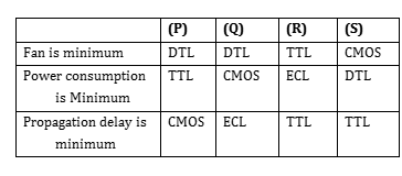
The correct column is
(GATE 2003 || EC || MCQ || 1 MARK)
P
Q
R
S
Question 7
The output of the 74 series GATE of TTL gates is taken from a BJT in
(GATE 2003 || EC || MCQ || 1 MARK)
Totem pole and common collector configuration.
Either totem pole or open collector configuration
Common base configuration
Common collector configuration
Question 8
A 3-input majority logic gate has inputs X, Y, and Z. The output F of the gate is logic '1' if two or more of the inputs are logic '1'. The output F is logic '0' if two or more of the inputs are logic '0'. Which one of the following options is a Boolean expression of the output F?
(GATE 2005 || EC || MCQ || 1 MARK)
XY + YZ + ZX
[Tex]X \oplus Y \oplus Z[/Tex]
X + Y + Z
XYZ
Question 9
For the circuit shown below, the propagation delay of each NAND gate is 1 ns. The critical path delay, in ns, is __________ (rounded off to the nearest integer).
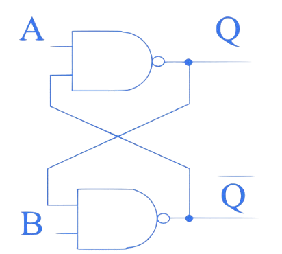
(GATE 2023 || EC || NAT ||1 MARK)
2
Question 10
Consider a Boolean gate (D) where the output Y is related to the inputs A and B as [Tex]Y = A + \overline{B}[/Tex] where + denotes the logical OR operation. The Boolean inputs ‘0’ and ‘1’ are also available separately. Using only D gates and these constant inputs, which of the following logic functions can or cannot be implemented?
(GATE 2022 || EC || MCQ ||1 MARK)
NAND logic can be implemented
OR logic cannot be implemented
NOR logic can be implemented
AND logic cannot be implemented
There are 10 questions to complete.