- Courses
- Tutorials
- Interview Prep
GATE EC ||DIGITAL LOGIC || LOGIC GATE AND MINIMIAZATION
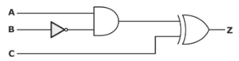
Question 1
In the circuit shown in the figure, if C = 0, what is the expression for Y?
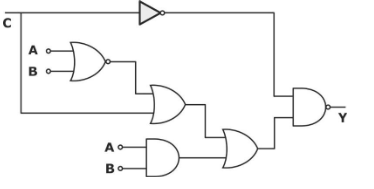
( GATE 2013 || EC || PYQ || MCQ || 1 MARK)
[Tex]Y = A\overline{B} + \overline{A}B[/Tex]
[Tex]Y = A + B[/Tex]
[Tex]Y = \overline{A + B}[/Tex]
[Tex]Y = AB[/Tex]
Question 2
The logic gates are shown in the digital circuit below use A-down n MOS transistors for LOW logic level at the outputs. When the pull-downs are off, high-value resistors set the output logic levels to HIGH (i.e., the pull-ups are weak). Note that some nodes are intentionally shorted to will be HIGH only if the output of all the gates whose outputs are shorted are HIGH.
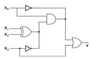
The number of distinct values of X3X2X1X0 (out of the 16 possible values) that give Y = 1 is
( GATE 2014 || EC || PYQ || NAT || 2 MARK)
8
Question 3
The output of the combinational circuit given below is
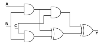
( GATE 2016 || EC || PYQ || MCQ || 1 MARK)
A + B + C
A(B+C)
B(C+A)
C(A+B)
Question 4
The minimum number of 2-input NAND gates required to implement a 2-input XOR gate is
( GATE 2016 || EC || PYQ || MCQ ||1 MARK)
4
5
6
7
Question 5
A universal logic gate can implement any Boolean function by connecting the sufficient number of them appropriately. Three gates are shown.
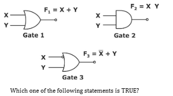
( GATE 2015 || EC || PYQ || MCQ || 1 MARK )
Gate 1 is a universal gate
Gate 2 is a universal gate
Gate 3 is a universal gate
None of the gates shown is a universal gate
Question 6
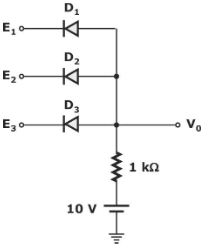
In the circuit shown, diodes D1, D2 and D3 are ideal. And the inputs E1, E2, and E3 are ‘0V’ for logic ‘0’ and ’10 V’ for logic ‘1’. What logic gate does the circuit represent?
( GATE 2015 || EC || PYQ || MCQ || 1 MARK)
3 input OR gate
3 input NOR gate
3 input AND gate
3 input XOR gate
Question 7
All the logic gates shown in the figure have a propagation delay of 20 ns. Let A = C = 0 and B = 1 at time t = 0. At t = 0, all the inputs change state simultaneously (i.e., A = C = 1 and B = 0) and remain in that state. For t > 0, the output Z becomes 1 for a duration of ___ ns.
( GATE 2015 || EC || PYQ || MCQ || 1 MARK )
40
Question 8
In the circuit shown in the figure, if C = 0, the expression for Y is

( GATE 2014 || EC || PYQ || MCQ || 2 MARK )
Y = A B̄ + Ā B
Y = A + B
Y = Ā + B̄
Y=AB
Question 9
The output F in the digital logic circuit shown in the figure is
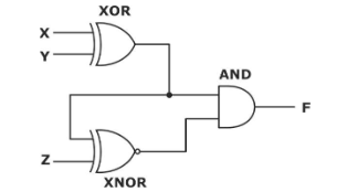
( GATE 2014 || ECE || PYQ || MCQ || 2 MARK )
F = X̄YZ + XȲZ
F = XȲZ + XYZ̄
F = X̄YZ + XYZ
F = X̄YZ + XYZ
Question 10
For the ring oscillator shown in the figure, the propagation delay of each inverter is 100 pico sec. What is the fundamental frequency of the oscillator output?
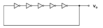
( GATE 2001 || EC || PYQ || MCQ || 1 MARK)
10 MHz
100MHz
2 GHz
1 GHz
There are 18 questions to complete.