- Courses
- Tutorials
- Interview Prep
GATE EC || DIGITAL LOGIC || SEQUENTIAL CIRCUIT || PYQS (2000-2025)
Question 1
For the circuit shown in the figure, the delay of the bubbled NAND gate is 2 ns, and that of the counter is assumed to be zero.
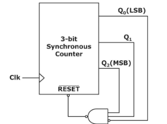
If the clock (Clk) frequency is 1 GHz, then the counter behaves as a
( GATE 2015 || EC || MCQ || 1 MARK )
mod-5 counter
mod-6 counter
mod-7 counter
mod-8 counter
Question 2
Five JK flip-flops are cascaded to form the circuit shown in the figure. Clock pulses at a frequency of 1 MHz are applied as shown. The frequency (in kHz) of the waveform at Q3 is:
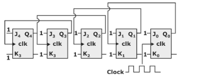
( GATE 2014 || EC || MCQ || 1 MARK )
(62.4 to 62.6)
Question 3
In the circuit shown, choose the correct timing diagram of the output (Y) from the given waveforms W1, W2, W3 and W4
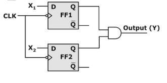
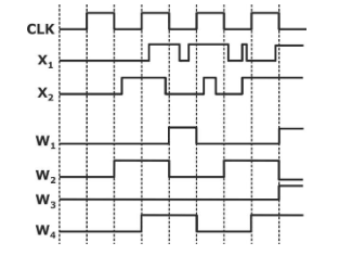
(GATE 2014 || EC || MCQ ||1 MARK)
W1
W2
W3
W4
Question 4
The outputs of the two flip-flops Q1, Q2 in the figure shown are initialized to 0, 0. The sequence generated at Q1 upon application of clock signal is
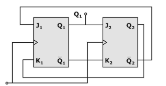
(GATE 2014 || EC || MCQ || 1 MARK)
01110
01010
00110
01100
Question 5
- Toggle flip-flop
- JK flip-flop
- SR Latch
- Master-Slave D flip-flop
Question 6
A mod-n counter using a synchronous binary up-counter with synchronous clear input is shown in the figure. The value of n is: ( GATE 2014 || EC || NAT || 1 MARK )
7
Question 7
The figure shows a binary counter with synchronous clear input. With the decoding logic shown, the counter works as a
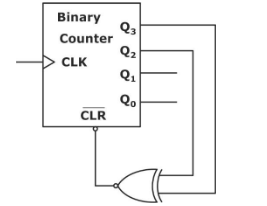
(GATE 2015 || EC || MCQ || 1 MARK)
mod-2 counter
mod-4 counter
mod-5 counter
mod-6 counter
Question 8
- a modulo-5 binary up counter
- a modulo-6 binary down counter
- a modulo-5 binary down counter
- a modulo-6 binary up counter
Question 9
An SR latch is implemented using TTL gates, as shown in the figure. The set and reset pulse inputs are provided using the push-button switches. It is observed that the circuit fails to work as desired. The SR latch can be made functional by changing
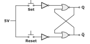
(GATE 2015 || EC || MCQ || 1 MARK)
NOR gates to NAND gates
Inverters to buffers
NOR gates to NAND gates and inverters to buffers
5V to ground
Question 10
A three-bit pseudo-random number generator is shown. Initially, the value of output Y = Y2Y1Y0 is set to 111. The value of output Y after three clock cycles is
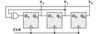
( GATE 2015 || EC || MCQ || 1 MARK)
000
001
010
100
There are 41 questions to complete.