- Courses
- Tutorials
- Interview Prep
GATE EC || ELECTRONIC DEVICES AND CIRCUIT || FET || PYQS (2000-2025)
Question 1
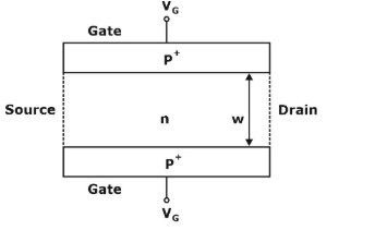
The cross-section of a JFET is shown in the following figure. The gate voltage is VG = –2V and let Vp be the initial pinch-off voltage. If the width W is doubled , while all other geometrical parameters and doping levels remain unchanged, determine the ratio of the mutual transconductances of the initial JFET to that of the modified JFET.
( GATE 2017 || EC || MCQ || 1 MARK)
4
[Tex]\frac{1}{2} \left( \frac{1 - \sqrt{\frac{2}{V_p}}}{1 - \sqrt{\frac{1}{2V_p}}} \right)[/Tex]
[Tex]\frac{1 - \sqrt{\frac{2}{V_p}}}{1 - \sqrt{\frac{1}{2V_p}}}[/Tex]
[Tex]\frac{1 - \sqrt{\frac{2}{V_p}}}{1 - \left(\frac{1}{2\sqrt{V_p}}\right)}[/Tex]
Question 2
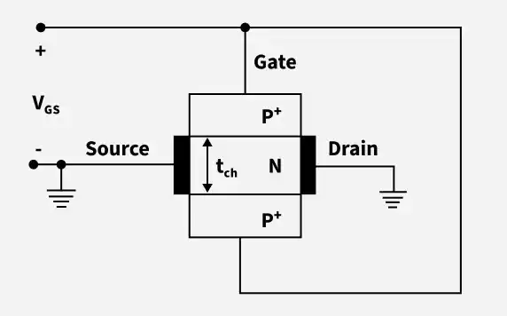
An N-channel JFET has a channel resistance of 600Ω when the entire channel thickness tch = 10 µm is available for conduction. The built-in potential of the gate p-n junction is Vbi = −1 V. When the gate-to-source voltage VGS = 0 V, the depletion region extends by 1 μm from each side of the channel due to the built-in potential, reducing the effective conducting channel thickness to 8 μm.

The channel resistance when VGS = 0 V is
(GATE 2011 || EC || MCQ || 2 MARK)
480Ω
600Ω
750Ω
1000Ω
Question 3
The channel resistance of an N-channel JFET shown in the figure below is 600Ω when the full channel thickness tch of 10μm is available for conduction. The built-in voltage of the gate P+-N junction (Vbi) is -1V. When the gate-to-source voltage (VGS) is 0 V, the channel is depleted by 1μm on each side due to the built-in voltage, and hence the thickness available for conduction is only 8μm.
The channel resistance when VGS = -3 V is?
(GATE 2011 || EC || MCQ || 2 MARK)
360 Ω
917 Ω
1000 Ω
3000 Ω
Question 4
An NMOS transistor operating in the linear region has IDS of 5μA at VDS of 0.1 V . Keeping VGS constant, the VDS is increased to 1.5 V. Given that μnCoxWL=50μA/V2, the transconductance at the new operating point (in μA/V, rounded off to two decimal places) is
(GATE 2024 || EC || NAT||1 MARK)
52.4 to 52.6
Question 5
Which of the following statements is/are true for a BJT with respect to its DC current gain β ?
(GATE 2024 || EC || MCQ || 1 MARK)
Under high-level injection condition in forward active mode, β will decrease with increase in the magnitude of collector current.
Under low-level injection condition in forward active mode, where the current at the emitter-base junction is dominated by recombination-generation process, β will decrease with increase in the magnitude of collector current.
β will be lower when the BJT is in saturation region compared to when it is in active region.
A higher value of β will lead To a lower value of the collector-to-emitter breakdown voltage
Question 6
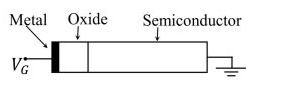
An ideal MOS capacitor (p-type semiconductor) is shown in the figure. The MOS capacitor is under strong inversion with VG=2VVG=2V. The corresponding inversion charge density QINQIN is 2.2μC/cm22.2μC/cm2. Assume oxide capacitance per unit area as COX=1.7μF/cm2COX=1.7μF/cm2. For VG=4VVG=4V, the value of QINQIN is ______μC/cm2μC/cm2 (rounded off to one decimal place).
(GATE 2017 || EC || MCQ||1 MARK)
-5.6
Question 7
An n-channel JFET has IDSS =12 mA and pinch-off voltage VP =−6 V. The drain current at VGS = −3 V is:
(GATE 2015 || EC || MCQ || 1 MARK)
3 mA
6 mA
6 mA
12 mA
Question 8
The input impedance of a JFET is very high because:
(GATE 2011 || EC || MCQ || 1 MARK)
Gate-source junction is forward biased
Gate-source junction is reverse biased
Drain current is zero
Source resistance is large
Question 9
An n-channel JFET has IDSS = 10 mA, VP = −5 V. The device is biased at VGS = −2 V. The transconductance gm is closest to:
(GATE 2008 || EC || MCQ || 2 MARK)
1.2 mS
2.4 mS
4 mS
8 mS
There are 9 questions to complete.