- Courses
- Tutorials
- Interview Prep
GATE EC|| ELECTRONIC DEVICES AND CIRCUIT ||MOSFET ||PYQS(2000-2025)
Question 1
Assuming that transistors M1 and M2 are identical and have a threshold voltage of 1V, the state of transistors M1 and M2 are respectively.
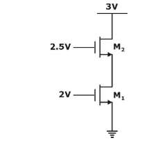
(GATE 2017 || EC || MCQ ||1 MARK)
Saturation, Saturation
Linear, Linear
Linear, Saturation
Saturation, Linear
Question 2
If fixed positive charges are present in the gate oxide of an n-channel enhancement type MOSFET. it will lead to
(GATE 2014 || EC || MCQ||1 MARK)
A. a decrease in the threshold voltage.
B. channel length modulation.
C. an increase in substrate leakage current
an increase in accumulation capacitance
Question 3
The source of a silicon (ni = 10^10 per cm^3) n-channel MOS transistor has an area of 1 μm^2 and a depth of 1 μm. If the dopant density in the source is 10^19 per cm^3, the number of holes in the source region with the above volume is approximately ______.
(GATE 2012 || EC || MCQ||1 MARK)
10 7
100
10
0
Question 4
Consider an n-channel metal oxide semiconductor field effect transistor (MOSFET) with a gate-to-source voltage of 1.8V. Assume that
[Tex]\frac{W}{L}[/Tex][Tex]\frac{W}{L} = 4, \quad \mu_n C_{ox} = 70 \times 10^{-6} \text{ A/V}^2[/Tex], the threshold voltage is 0.3 V and the channel length modulation parameter is 0.09
. In the saturation region, the drain conductance (in micro Siemens) is
(GATE 2016 || EC || MCQ||1 MARK)
28
Question 5
Given transistor is in saturation region, and
Current = 1 mA at VDS = 5 V
Current = 1.02 mA at VDS = 6 V
Assuming VG constant, current in saturation region is
[Tex]I_D = \frac{k}{2} (V_{GS} - V_{TN})^2 (1 + \lambda V_{DS})[/Tex]
[Tex]I_{D_1} = (1 + \lambda V_{DS_1})[/Tex]
[Tex]I_{D_2} =(1 + \lambda V_{DS_2})[/Tex]
[Tex]\text{So, } \frac{1.02\text{mA}}{1\text{mA}} = \frac{(1 + \lambda V_{DS_2})}{(1 + \lambda V_{DS1})}[/Tex]
[Tex]1.02 = \frac{1 + 6\lambda}{1 + 5\lambda}[/Tex]
[Tex]\lambda = 0.022 \text{V}^{-1}[/Tex]
Alternate solution:
[Tex]\frac{\partial I_D}{\partial V_{DS}} = \frac{1}{r_0} = \lambda I_{Dsat}[/Tex]
[Tex]r_0 = \frac{1\text{mA} - 1.02\text{mA}}{6\text{V} - 5\text{V}} = \lambda \cdot 1\text{mA} \implies \lambda = 0.02\text{V}^{-1}[/Tex]
(GATE 2015 || EC || MCQ||1 MARK)
Question 6
The current in an enhancement mode NMOS transistor biased in saturation mode was measured to be 1 mA at a drain-source voltage of 5 V. When the drain-source voltage was increased to 6 V while keeping gate-source voltage same, the drain current increased to 1.02 mA. Assume that drain to source saturation voltages is much smaller than the applied drain-source voltage. The channel length modulation parameter λ (V–1) is.
( GATE 2015 || EC || NAT||1 MARK)
0.02
Question 7
Consider an n-channel metal oxide semiconductor field effect transistor (MOSFET) with a gate-to-source voltage of 1.8V. Assume that W/L = 4, μnCox = 70 × 10–6 A-V–2, the threshold voltage is 0.3 V and the channel length modulation parameter is 0.09. In the saturation region, the drain conductance (in micro Siemens) is V-1
(GATE 2017 || EC || MCQ||1 MARK)
28 to 29
Question 8
A long-channel NMOS transistor is biased in the linear region with VDS = 50 mV and is used as a resistance. Which one of the following statements is NOT correct?
(GATE 2017 || EC || MCQ||1 MARK)
If the device width W is increased, the resistance decreases.
If the threshold voltage is reduced, the resistance decreases.
If the device length L is increased, the resistance increase.
If VGS is increased, the resistance increases.
Question 9
Consider the following statements for a metal oxide semiconductor field effect transistor (MOSFET):
P: As channel length reduces, OFF-state current increases.
Q: As channel length reduces, output resistance increases.
R: As channel length reduces, threshold voltage remains constant.
S: As channel length reduces, ON current increases.
Which of the above statements are INCORRECT?
(GATE 2017 || EC || MCQ||1 MARK)
P and Q
P and S
Q and R
R and S
Question 10
(1.18 to 1.22)
Since VGS> VDS,
MOSFET is in linear operation
ID = KN [VGS – VT] VDS(neglecting V2DS/2 term )
![]() = KN VDS
= KN VDS
gm = KN VDS
0.5 × 10–5 = KN [50 × 10–3]
KN = 10–5
ID = KN [VGS –VT] VDS
![]() = KN [VGS – VT]
= KN [VGS – VT]
gd = KN [VGS – VT]
8 ×10–6 = 10–5 [2 –VT]
![]() 2 – VT
2 – VT
8 × 10–1 = 2 – VT
0.8 = 2 – VT
![]() VT = 1.2 V
VT = 1.2 V
Hence threshold voltage of the transistor is 1.2 V.
26. (1.9 to 2.1)
(1.18 to 1.22)
There are 21 questions to complete.