- Courses
- Tutorials
- Interview Prep
GATE EC || ELECTRONIC DEVICES AND CIRCUIT || PN JUNCTION DIODE || PYQS (2000-2025)
Question 1
Consider avalanche breakdown in a silicon p+n junction. The n-region is uniformly doped with a donor density ND. Assume that breakdown occurs when the magnitude of the electric field at any point in the device becomes equal to the critical field Ecrit. Assume Ecrit to be independent of ND. If the built-in voltage of the p+n junction is much smaller than the breakdown voltage, VBR, the relationship between VBR and ND is given by
( GATE 2016 || EC || MCQ||1 MARK)
VBR ×

= constant
ND ×

= constant
ND × VBR = constant
ND/VBR = constant
Question 2
The photocurrent of a PN junction diode solar cell is 1 mA. The voltage corresponding to its maximum power point is 0.3 V. If the thermal voltage is 30mV, the reverse saturation current of the diode (in nA, rounded off to two decimal places) is
(GATE 2024 || EC || NAT||1 MARK)
4.13
Question 3
An ideal p-n junction germanium diode has a reverse saturation current of 10μ A at 300 K .The voltage (in Volts, rounded off to two decimal places) to be applied across the junction to get a forward bias current of 100 mA at 300 K is __________ (Consider the Boltzmann constant kB=1.38×10⁻²³ J/K and the charge of an electron e=1.6×10⁻¹⁹C.)
(GATE 2025 || EC || NAT||1 MARK)
0.23
Question 4
The phenomenon known as “Early Effect” in a bipolar transistor refers to a reduction of the effective base-width caused by
(GATE 2006 || EC || MCQ||1 MARK)
electron-hole recombination at the base
the reverse biasing of the base-collector junction
the forward biasing of emitter-base junction
the early removal of stored base charge during saturation to-cut-off switching
Question 5
Consider the following statements S1 and S2.
S1: The β of a bipolar transistor reduces if the base width is increased.
S2: The β of a bipolar transistor increases if the doping concentration in the base is increased.
Which one of the following is correct?
(GATE 2004 || EC || MCQ||1 MARK)
S1 is FALSE and S2 is TRUE
Both S1 and S2 are TRUE
Both S1 and S2 are FALSE
S1 and TRUE and S2 is FALSE
Question 6
If for a silicon n-p-n transistor, the base-to- emitter voltage (VBE) is 0.7 V and the collector to base voltage (VCB) is 0.2V, then the transistor is operating in the
(GATE 2004 || EC || MCQ||1 MARK)
normal active mode
saturation mode
inverse active mode
cutoff mode
Question 7
The neutral base width of a bipolar transistor, biased in the active region, is 0.5 μm. The maximum electron concentration and the diffusion constant in the base are 1014/cm3 and Dn = 25 cm2/sec respectively in the base, the collector current density is (the electron charge is 1.6 × 10⁻¹⁹ Coulomb)
(GATE 2004 || EC || MCQ|| 1 MARK)
800 A/cm2
8 A/cm2
200 A/cm2
2 A/cm2
Question 8
The impurity commonly used for realizing the base region of a silicon n-p-n transistor is
(GATE 2014 || EC || MCQ||1 MARK)
Gallium
Indium
Boron
Phosphorus
Question 9
A one-sided abrupt p-n junction diode has a depletion capacitance CD of 50 PF at reverse bias of 0.2 V. The plot of 1/CD2 versus the applied voltage V for this diode is a straight line as shown in the below. The slope of the plot is ......... × 1020 F–2V–1
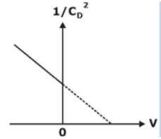
(GATE 2020 || EC || MCQ || 1 MARK)
–0.47
–5.7
insufficient data
–3.8
Question 10
A silicon P-N junction is shown in the figure. The doping in the P region is 5 × 1016 cm-3 and doping in the N region is 10 × 1016 cm-3. The parameters given are
Built-in voltage(Φbi) = 0.8 V
Electron charge (q) = 1.6 x 10⁻¹⁹ C
Vacuum permittivity (ε0) = 8.85 × 10⁻¹² F/m
Relative permittivity of silicon (εSi) = 12

The magnitude of reverse bias voltage that would completely deplete one of the two regions (P or N) prior to the other (rounded off to one decimal place) is ____ V.
(GATE 2021 || EC || NAT||1 MARK)
8.24
There are 31 questions to complete.