- Courses
- Tutorials
- Interview Prep
GATE EC || ELECTRONIC DEVICES AND CIRCUIT || SEMICONDUCTORS || PYQS (2000-2025)
Question 1
The I-V characteristics of three types of diodes at the room temperature, made of semiconductors X, Y and Z, are shown in the figure. Assume that the diodes are uniformly doped and identical in all respects except their materials. If EgX, EgY and EgZ are the band gaps of X, Y and Z, respectively, then
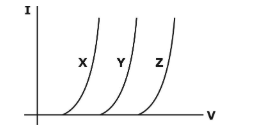
( GATE 2016 || EC || MCQ ||1 MARK)
EgX > EgY > EgZ
EgX = EgY = EgZ
EgX < EgY < EgZ
no relationship among these band gaps exists
Question 2
The figure below shows the doping distribution in a p-type semiconductor in log scale
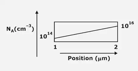
The magnitude of the electric field (in kV/cm) in the semiconductor due to non uniform doping
( GATE 2016 || EC || NAT ||1 MARK)
1.19
Question 3
Consider a silicon sample at T = 300 K, with a uniform donor density Nd = 5 × 1016 cm–3 illuminated uniformly such that the optical generation rate is Gopt = 1.5 × 1020 cm–3 S–1 throughout the sample. The incident radiation is turned off at t = 0. Assume low-level injection to be valid and ignore surface effects. The carrier lifetimes are ![]() = 0.1 μs and
= 0.1 μs and ![]() = 0.5 μs
= 0.5 μs
The hole concentration at t = 0 and the hole concentration at t=0.3μs, respectively, are
(GATE 2016 || EC || MCQ ||1 MARK)
1.5 × 1013 cm–3 and 7.47 × 1011 cm–3
1.5 × 1013 cm–3 and 8.23 × 1011 cm–3
7.5 × 1013 cm–3 and 3.73 × 1011 cm–3
7.5 × 1013 cm–3 and 4.12 × 1011 cm–3
Question 4
A bar of Gallium Arsenide (GaAs) is doped with Silicon such that the Silicon atoms occupy Gallium and Arsenic sites in the GaAs crystal. Which one of the following statements is true?
(GATE 2017 || EC || MCQ ||1 MARK)
Silicon atoms act as p-type dopants in Arsenic sites and n-type dopants in Gallium sites.
Silicon atoms act as n-type dopants in Arsenic sites and p-type dopants in Gallium sites.
Silicon atoms act as p-type dopants in Arsenic as well as Gallium sites.
Silicon atoms act as n-type dopants in Arsenic as well as Gallium sites.
Question 5
The dependence of drift velocity of electrons on electric field in semiconductor is shown below. The semiconductor has a uniform electron concentration of n = 1 × 1016 cm3 and electronic charge q = 1.6 × 10⁻¹⁹ C. If a bias of 5 V is applied across a 1 μm region of this semiconductor, the resulting current density in this region, in kA/cm2 is ____.
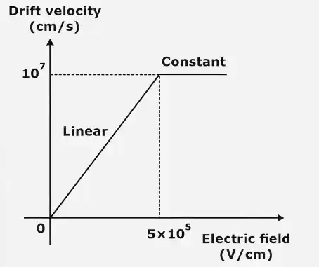
(GATE 2017 || EC || NAT ||1 MARK)
1.6
Question 6
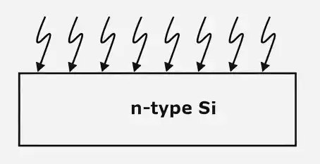
As shown, a uniformly doped Silicon (Si) bar of length
L = 0.1μm with a donor concentration ND =1016 cm-3 is illuminated at x =0 such that electron and hole pairs are generated at the rate of
[Tex]GL = G L_0 \left(1 - \frac{x}{L}\right), \quad 0 \le x \le L[/Tex]
where GL0 = 1017 cm–3 s–1. Hole lifetime is 10–4s, electronic charge q = 1.6 × 10⁻¹⁹C, hole diffusion coefficient Dp = 100 cm2/s and low-level injection condition prevails. Assuming a linearly decaying steady state excess hole concentration that goes to 0 at x = L, the magnitude of the diffusion current density at x = L/2, in A/cm2, is ____.
( GATE 2017 || EC || NAT ||1 MARK)
16
Question 7
A Germanium sample of dimension 1 cm × 1 cm is illuminated with a 20 mW, 600 nm laser light source as shown in the figure. The illuminated sample surface has a 100 nm of loss-less Silicon dioxide layer that reflects one-fourth of the incident light, From the remaining light, one-third of the power is reflected form the silicon dioxide- Germanium interface, one-third is absorbed in the Germanium layer, and one-third is transmitted through the other side of the sample. If the absorption coefficient of Germanium at 600 nm is 3 × 104 cm–1 and the band gap is 0.66 eV, the thickness of the Germanium layer, rounded off to 3 decimal places, is ___ μm
(GATE 2019 || EC || NAT ||1 MARK)
0.231
Question 8
A single crystal intrinsic semiconductor is at temp of 300 K with effective density of states for holes twice that of electrons. VT = 26mV. The intrinsic Fermi level is shifted from mid band gap energy level by
( GATE 2020 || EC || MCQ ||1 MARK)
13.45 meV
18.02 meV
26.90 meV
9.01 meV
Question 9
Consider the recombination process via bulk traps in a forward biased p-n homojunction diode. The maximum recombination rate is Umax. If the electron and the hole capture cross-sections are equal, which one of the following is FALSE?
(GATE 2020 || EC || MCQ ||1 MARK)
With all other parameters unchanged, Umax decreases if the intrinsic carrier density is reduced.
Umax occurs at the edges of the depletion region in the device.
Umax depends exponentially on the applied bias.
With all other parameters unchanged, Umax increases if the thermal velocity of the carriers increases.
Question 10
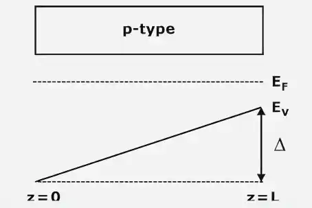
The energy band diagram of a p-type semiconductor bar of length L under equilibrium condition (i.e., the Fermi energy level EF is constant) is shown in the figure. The valance band EV is sloped since doping is non-uniform along the bar. The difference between the energy levels of the valence at the two edges of the bar is Δ. If the charge of an electron is q, then the magnitude of the electric filed developed inside this semiconductor bar is

( GATE 2021 || EC || MCQ || 1 MARK)
[Tex]\frac{2\Delta}{qL}[/Tex]
[Tex]\frac{3\Delta}{2qL}[/Tex]
[Tex]\frac{\Delta}{2qL}[/Tex]
[Tex]\frac{\Delta}{qL}[/Tex]
There are 63 questions to complete.