- Courses
- Tutorials
- Interview Prep
GATE EC || ELECTRONICDEVICES AND CIRCUIT || MOS CAPACITOR || PYQS (2000-2025)
Question 1
A MOS capacitor made using p-type substrate is in the accumulation mode. The dominant charge in the channel is due to the presence of
(GATE 2005|| EC || MCQ ||1 MARK)
holes
electrons
positively charged ions
negatively charged ions
Question 2
The figure shows the high-frequency capacitance-voltage (C-V) characteristics of a Metals/SiO₂/silicon (MOS) capacitor having an area of 1 × 10⁻⁴ cm². Assume that the permittivities (ε₀εᵣ) of silicon and SiO₂ are 1 × 10⁻¹² F/cm and 3.5 × 10⁻¹³ F/cm respectively. The gate oxide thickness in the MOS capacitor is
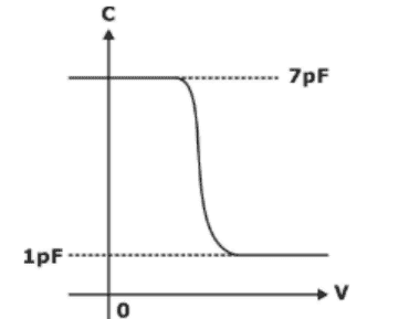
(GATE 2007 || EC || MCQ|| 2 MARK)
50 nm
143 nm
350 nm
1 μm
Question 3
The figure shows the high-frequency capacitance–voltage (C–V) characteristics of a [Tex]\text{Metal/SiO}_2\text{/Silicon (MOS)}[/Tex] capacitor having an area of [Tex]1 \times 10^{-4}\ \text{cm}^2[/Tex]. Assume that the permitivities [Tex](\varepsilon_0 \varepsilon_r)[/Tex] of silicon and [Tex]\text{SiO}_2[/Tex] are [Tex]1 \times 10^{-12}\ \text{F/cm} \quad \text{and} \quad 3.5 \times 10^{-13}\ \text{F/cm}[/Tex], respectively.
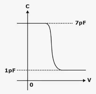
The maximum depletion layer width in Silicon is
(GATE 2007 || EC || MCQ || 2 MARK)
1.143 μm
0.857 μm
1 μm
1.143 μm
Question 4
In the three-dimensional view of a silicon n-channel MOS transistor shown below, δ=20nm. The transistor has a width of 1μm. The depletion width formed at every p–n junction is 10nm. The relative permitivities of Si and [Tex]\text{SiO}_2[/Tex] are 11.7 and 3.9, respectively, and [Tex]\varepsilon_0 = 8.9 \times 10^{-12}\ \text{F/m}[/Tex]

The source-body junction capacitance is approximately
(GATE 2022 || EC || MCQ || 1 MARK)
2 fF
7 fF
2 pF
7 pF
Question 5
An ideal MOS capacitor has boron doping concentration of 1015 cm–3 in the substrate. When a gate voltage is applied, a depletion region of width 0.5 μm is formed with a surface (channel) potential of 0.2 V.
Given that ε0 = 8.854 × 10⁻¹⁴ F/cm and the relative permittivity’s of silicon and silicon dioxide are 12 and 4, respectively, the peak electric field (in V/μm) in the oxide region is ____.
(GATE 2014 || EC || NAT||1 MARK)
(2.3 to 2.5)
Question 6
In a MOS capacitor with an oxide layer thickness of 10 nm, the maximum depletion layer thickness is 100 nm. The permittivities of the semiconductor and the oxide layer are 𝜀𝑠 and 𝜀𝑂𝑆 respectively. Assuming 𝜀𝑠/𝜀𝑂𝑋 = 3, the ratio of the maximum capacitance to the minimum capacitance of this MOS capacitor is.
(GATE 2014 || EC || NAT||1 MARK)
(4.3 to 4.4)
Question 7
The figure shows the band diagram of a Metal Oxide Semiconductor (MOS). The surface region of this MOS is in
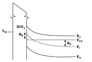
(GATE 2016|| EC || MCQ || 1 MARK)
inversion
accumulation
depletion
flat band
Question 8
Figure I and II show two MOS capacitors of unit area. The capacitor in Figure I has insulator materials X (of thickness t1 = 1 nm and dielectric constant ε1 = 4) and Y (of thickness t2 = 3 nm and dielectric constant ε2 = 20). The capacitor in Figure II has only insulator material X of thickness teq. If the capacitors are of equal capacitances, then the value of tEq (in nm) is _____.
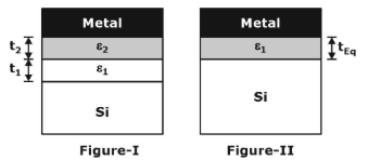
(GATE 2016|| EC || MCQ ||1 MARK)
(1.55 to 1.65)
Question 9
A voltage VG is applied across a MOS capacitor with metal gate and p-type Silicon substrate at T = 300 K. The inversion carrier density (in number of carriers per unit area) for VG = 0.8 V is 2 × 1011 cm–2. For VG = 1.3 V, the inversion carrier density is 4 × 1011 cm–2. For VG = 1.3 V, the inversion carrier density is 4 × 1011cm–2. What is the value of the inversion carrier density for VG = 1.8 V?
(GATE 2016 || EC || MCQ || 2 MARK)
4.5 ×1011 cm–2
6.0 ×1011 cm–2
7.2 ×1011 cm–2
8.4 ×1011 cm–2
Question 10
The band diagram of a p-type semiconductor with a band -gap of 1eV is shown, using this semiconductor, a MOS capacitor having Vth of -0.16 V, C’ox of 100 nF/cm2 and a metal work function of 3.87 eV is fabricated. There is no charge within the oxide. If the voltage across the capacitor is VTH, the magnitude of depletion charge per unit area (in C/cm2) is
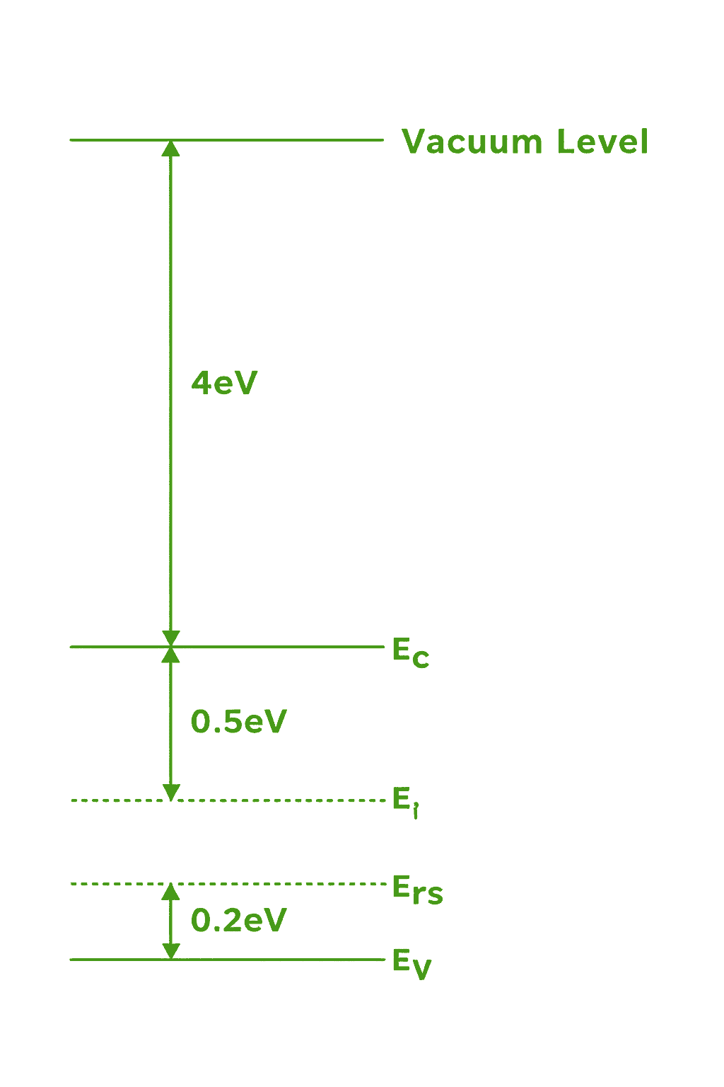
(GATE 2020 || EC || MCQ || 2 MARK)
0.52 × 10⁻⁸
0.93 × 10⁻⁸
1.41 × 10⁻⁸
1.70 × 10⁻⁸
There are 12 questions to complete.