- Courses
- Tutorials
- Interview Prep
GATE EC||ANALOG ELECTRONIC||BJT||PYQS(2000-2025)
Question 1
For the BJT Q1 in the circuit shown below, β = ∞, VBE(on) = 0.7 VCE(sat) = 0.7 V. The switch is initially closed. At time t = 0, the switch is opened. The time t at which Q1 leaves the active region is
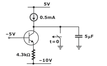
(GATE 2011|| EC || PYQ || MCQ || 2 MARKS)
10 ms
25 ms
50 ms
100 ms
Question 2
In the voltage regulator shown below, V1 is the unregulated at 15 V. Assume VBE = 0.7 V and the base current is negligible for both the BJTs. If the regulated output Vo is 9 V, the value of R2 is ……. Ω.
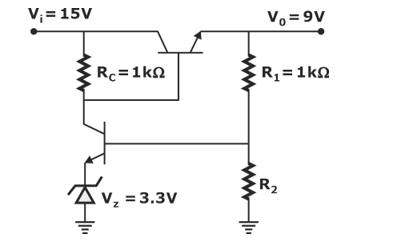
(GATE 2020 || EC || PYQ || NAT ||2 MARKS)
800
Question 3
In the figure shown, the npn transistor acts as a switch
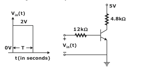
For the input Vin(t) as shown in the figure, the transistor switches between the cut-off and saturation regions of operation, when T is large. Assume collector-to-emitter voltage at saturation VCE(sat)= 0.2V and base-to-emitter voltage VBE = 0.7 V. The minimum value of the common- base current gain (α) of the transistor for the switching should be ………….
( GATE 2017 || EC || PYQ || NAT ||2 MARKS)
0.902
Question 4
Consider the circuit shown in the figure. Assuming VBE1 = VEB2 = 0.7 volt, the value of the dc voltage VC2 (in volt) is …………………..
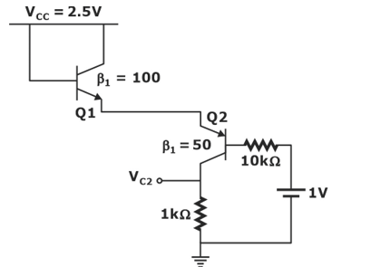
(GATE 2016 || EC || PYQ || NAT ||2 MARKS)
0.5
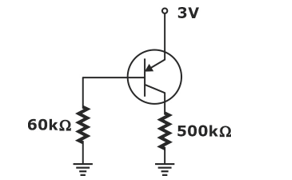
Question 5
The Ebers-Moll model of a BJT is valid
(GATE 2016 || EC || PYQ || MCQ ||2 MARKS)
only in a active mode
only in active and saturation modes
only in active and cut-off modes
in active, saturation and cut-off modes
Question 6
In the circuit shown in the figure, the BJT has a current gain (β) of 50. For an emitter base voltage VEB = 600 mV, the emitter collector voltage VEC (in Volts) is ……………….
(GATE 2015 || EC || PYQ || NAT ||1 MARKS)
2
Question 7
In the circuit shown, the silicon BJT has β = 50. Assume VBE = 0.7 V and VCE(sat) = 0.2V. Which one of the following statements is correct?
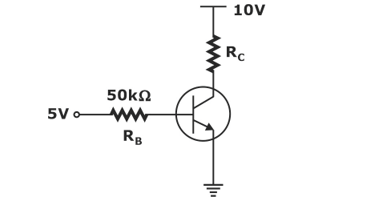
(GATE 2014|| EC || PYQ || MCQ || 2 MARKS)
For RC = 1 kΩ , the BJT operates in the saturation region
For RC = 1 kΩ , the BJT operates in the saturation region
For RC = 20 k Ω, the BJT operates in the saturation region
For RC = 20 kΩ, the BJT operates in the linear region
Question 8
In the circuit shown, the PNP transistor has |VBE| = 0.7 V and β = 50. Assume that RB = 100 k Ω. For V0 to be 5 V, the value of RC (in k Ω) is ………….. .
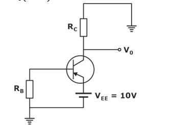
(GATE 2014|| EC || PYQ || NAT ||1 MARKS)
1.075
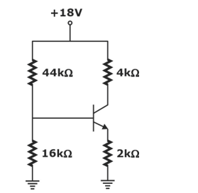
Question 9
In the circuit shown below, the silicon npn transistor Q has a very high value of β. The required value of R2 in kΩ to produce IC = 1 mA is

(GATE 2013|| EC || PYQ || MCQ || 2 MARKS)
20
30
40
50
Question 10
Consider the circuit shown in the figure. Assume base-to-emitter voltage VBE = 0.8 V and. Common- base current gain (α) of the transistor is unity. The value of collector-to-emitter voltage VCE (in Volt) is ………….
(GATE 2012|| EC || PYQ || NAT ||2 MARKS)
6
There are 22 questions to complete.