- Courses
- Tutorials
- Interview Prep
GATE EC||ANALOG ELECTRONIC||CURRENT MIRROR CIRCUIT||PYQS(2000-2025)
Question 1
For the circuit shown in the following figure, transistors M_1 and M_2 are identical NMOS transistors. Assume that M_2 is in saturation and the output is unloaded
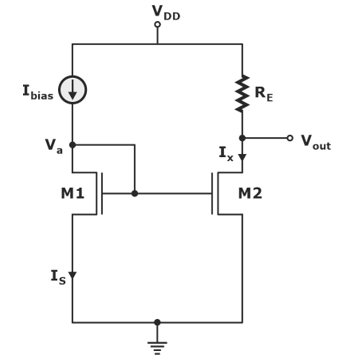
The current Ix is related to Ibias as
(GATE 2008 || EC || PYQ || MCQ || 2 MARKS)
IX = Ibias – IS
IX = Ibias
IX = Ibias – IS
I_x = I_{bias} - \left( V_{DD} - \frac{V_{out}}{R_E} \right)
Question 2
In the silicon BJT circuit shown below, assume that the emitter area of transistor Q1 is half that of transistor Q2.
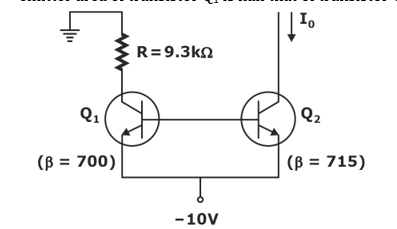
The value of current I0 is approximately
(GATE 2010 || EC || PYQ || MCQ || 1 MARKS)
0.5 mA
2 mA
9.3 mA
15 mA
Question 3
Resistor R1 in the circuit below has been adjusted so that I1 = 1 mA. The bipolar transistors Q1 and Q2 are perfectly matched and have very high current gain, so their base currents are negligible. The supply voltage Vcc is 6 V. The thermal voltage kT/q is 26 mV.

The value of R2 (in Ω) for which I2 = 100 μA is.
(GATE 2016 || EC || PYQ || NAT ||1 MARKS)
575.6
Question 4
In the circuit shown, V1 = 0 and V2 = Vdd. The other relevant parameters are mentioned in the figure. Ignoring the effect of channel length modulation and the body effect, the value of Iout is ___________ mA (rounded off to 1 decimal place).
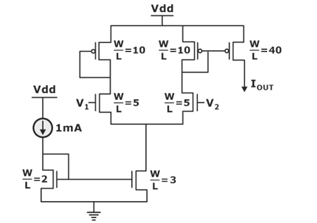
(GATE 2019 || EC || PYQ || NAT ||2 MARKS)
6
There are 4 questions to complete.