- Courses
- Tutorials
- Interview Prep
GATE EC||ANALOG ELECTRONIC||MOS||PYQS(2000-2025)
Question 1
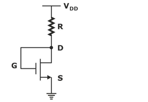
For the n-channel MOS transistor shown in the figure, the threshold voltage Vth is 0.8 V. Neglect channel length modulation effects. When the drain voltage VD = 1.6 V, the drain current ID was found to be 0.5 mA. If VD is adjusted to be 2 V by changing the values of R and VDD, the new value of ID (in mA) is
( GATE 2014 || EC || PYQ || MCQ || 2 MARKS)
0.625
0.75
1.125
1.5
Question 2
For the transistor M1 in the circuit shown in the figure, μnCOX = 100μA/V2 and (W/L) = 10, where μn is the mobility of electron. COX is the oxide capacitance per unit area. W is the width and L is the length.
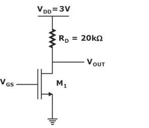
The channel length modulation coefficient is ignored. If the gate-to-source voltage VGS is 1V to keep the transistor at the edge of saturation, then the threshold voltage of the transistor (rounded off to one decimal place) is_____ V.
( GATE 2021 || EC || PYQ || NAT||2 MARKS)
0.5V
Question 3
In the circuit shown in the figure, the transistors M1 and M2 are operating in saturation. The channel length modulation coefficients of both the transistors are non-zero. The transconductance of the MOSFETs M1 and M2 are gm1 and gm2 respectively and internal resistance of MOSFETS M1 and M2 are r01 and r02, respectively.
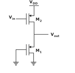
Ignoring the body effect, the ac small signal gain (∂Vout/∂Vin) of the circuit is
(GATE 2021 || EC || PYQ || MCQ || 1 MARKS)
[Tex]-g_{m2}(r_{o1} \parallel r_{o2})[/Tex]
[Tex]-g_{m2}\left(\frac{1}{g_{m1}} \parallel r_{o1} \parallel r_{o2}\right)[/Tex]
[Tex]-g_{m2}\left(\frac{1}{g_{m1}} \parallel r_{o2}\right)[/Tex]
[Tex]-g_{m1}\left(\frac{1}{g_{m2}} \parallel r_{o1} \parallel r_{o2}\right)[/Tex]
Question 4
Using the incremental low frequency small-signal model of the MOS device, the Norton equivalent resistance of the following circuit is
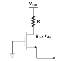
(GATE 2020 || EC || PYQ || MCQ || 2 MARKS)
[Tex]r_{ds} + R + g_m r_{ds}R[/Tex]
[Tex]\frac{r_{ds} + R}{1 + g_m r_{ds}}[/Tex]
[Tex]r_{ds} + R[/Tex]
[Tex]r_{ds} + \frac{1}{g_m} + R[/Tex]
Question 5
An enhancement MOSFET of threshold voltage 3V is being used in the sample and hold circuit given below. Assume that the substrate of MOS device is connected to –10V. If the input voltage V1 lies between ± 10V, the minimum and the maximum values of VG required of proper sampling and holding respectively, are
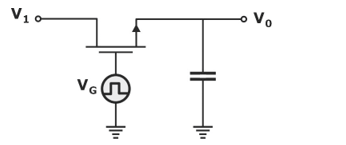
(GATE 2020 || EC || PYQ || MCQ || 2 MARKS)
10 V and -10 V
10 V and -13 V
13 V and -7V
3V and -3V
Question 6
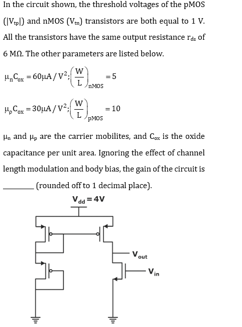
(GATE 2019 || EC || PYQ || NAT ||2 MARKS)
–900
Question 7
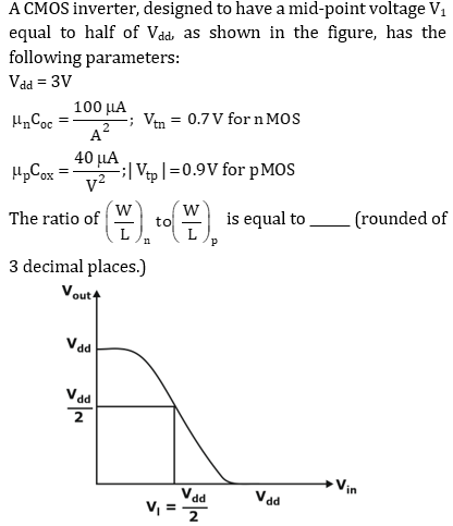
(GATE 2017 || EC || PYQ || NAT ||2 MARKS)
0.225
Question 8
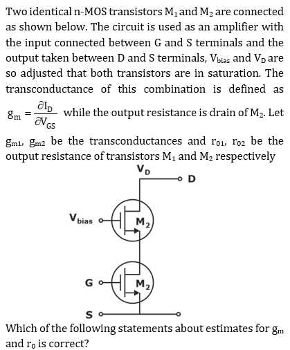
(GATE 2018 || EC || PYQ || MCQ ||1 MARKS)
gm = gm1. gm2. r02 and r0 = r01 + r02
gm = gm1 + gm2 and r0 = +r02
gm = gm1 and r0 = r01. gm2. r02
gm = gm1 and r0 = r02
Question 9
An n-channel enhancement mode MOSFET is biased at VGS > VTH and VDS > (VGS - VTH), where VGS is the gate-to-source voltage. VDS is the drain-to-source voltage and VTH is the threshold voltage. Considering channel length modulation effect to be significant, the MOSFET behaves as a
(GATE 2017 || EC || PYQ || MCQ ||1 MARKS)
voltage source with zero output impedance
voltage source with non-zero output impedance
current source with finite output impedance
current source with infinite output impedance
Question 10
In the circuit shown in the figure, the channel length modulation of all transistor is non-zero Also, all transistors operate in saturation and have negligible body effect. The ac small signal voltage gain (V0/Vin) of the circuit is
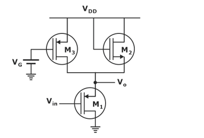
(GATE 2016 || EC || PYQ || MCQ || 2 MARKS)
[Tex]-g_{m1}(r_{o1} \parallel r_{o2} \parallel r_{o3})[/Tex]
[Tex]-g_{m1}\left(r_{o1} \parallel \frac{1}{g_{m3}} \parallel r_{o3}\right)[/Tex]
[Tex]-g_{m1}\left(r_{o1} \parallel \left(\frac{1}{g_{m2}} \parallel r_{o2}\right) \parallel r_{o3}\right)[/Tex]
[Tex]-g_{m1}\left(r_{o1} \parallel \left(\frac{1}{g_{m2}} \parallel r_{o3}\right) \parallel r_{o2}\right)[/Tex]
There are 26 questions to complete.