An Application-Specific Integrated Circuit (ASIC) is a custom-designed chip created to perform a specific function or set of functions. Unlike general-purpose processors, ASICs are optimized for a particular application, which allows them to deliver higher performance, lower power consumption, and smaller size for that task. ASICs are widely used in industries such as telecommunications, consumer electronics, automotive, and medical devices.
This article explains the fundamental concepts of ASIC design, covering what ASICs are, the different types of ASIC designs, the standard design flow, and key factors to consider during design. By the end, you will have a clear understanding of how ASICs are developed from concept to production.
Types of ASIC Designs
ASICs are categorized based on how much of the chip is customized and how they are designed. The main types include:
1. Full Custom ASIC
This type involves designing every transistor and circuit element from scratch. It offers the highest performance, lowest power consumption, and smallest area since everything is optimized for the specific application.
Example:
- High-performance microprocessors or graphics processing units (GPUs).
- Full custom design is time-consuming and expensive but delivers maximum efficiency.
2. Custom ASIC
Semi-custom ASICs use pre-designed building blocks to reduce design time and cost. They can be further divided into:
- Standard Cell ASICs: Uses a library of pre-made logic gates (AND, OR, flip-flops, etc.) called standard cells. Designers assemble these cells to create the desired circuit.
- Gate Array ASICs: Start with a prefabricated wafer containing an array of unconnected transistors or gates. Customization is done by creating metal interconnections to form the required logic.
Example:
- Networking chips or embedded controllers that balance performance and cost.
- Semi-custom ASICs reduce design cycles compared to full custom.
3. Structured ASIC
Structured ASICs have a predefined array of logic and transistors with fixed base layers. Customization is mainly in the metal interconnect layers. This design reduces both time-to-market and non-recurring engineering (NRE) costs while offering better optimization than gate arrays.
Example: Medium volume consumer electronics or telecommunications products.
4. Programmable ASICs (FPGA and PLDs)
These chips can be programmed after manufacturing, providing flexibility and fast prototyping.
- Field Programmable Gate Arrays (FPGAs): Large arrays of configurable logic blocks connected by programmable interconnects. Used in prototyping, development, and low-to-medium volume products.
- Programmable Logic Devices (PLDs): Smaller, simpler programmable chips often used for glue logic or simple functions.
Examples: Xilinx and Intel FPGAs, Altera devices.
Note: While highly flexible, programmable ASICs generally consume more power and have larger area compared to custom ASICs.
All types of ASICs are primarily fabricated using CMOS (Complementary Metal-Oxide-Semiconductor) technology. CMOS provides low power consumption, high noise immunity, and good scalability, making it the industry standard for integrated circuits
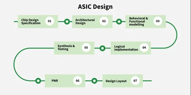
ASIC Design Flow
The ASIC design process consists of a series of well-defined steps that transform a concept into a physical chip ready for manufacturing. The main stages are:
- Specification: Define chip functionality, performance, power, and size requirements.
- Architecture Design: Create high-level block structure and data flow.
- RTL Design: Write hardware logic using Verilog or VHDL.
- Synthesis: Convert RTL code into gate-level netlist.
- Physical Design: Floorplan, place, and route to create chip layout.
- Verification: Simulate and analyse timing to ensure correctness.
- Fabrication: Manufacture the chip at a semiconductor foundry.
Each step is critical to ensure the final chip meets the intended specifications and performance.
 ASIC Design Flow
Key Considerations in ASIC Design
- Performance: The ASIC must meet the required speed and processing power to handle its intended tasks efficiently. This involves optimizing the design to reduce critical path delays and ensure reliable operation at the target clock frequency.
- Power Consumption: Minimizing power use is crucial for reducing heat generation and extending battery life in portable devices. Power optimization includes techniques like clock gating, voltage scaling, and efficient logic design to manage both dynamic and static power.
- Area: A smaller chip area reduces manufacturing costs and increases yield, as more chips fit on a silicon wafer. Efficient layout and design optimizations help minimize the physical size without compromising performance.
- Cost: Cost depends on design complexity, fabrication technology, and production volume. Designers must balance upfront design and mask costs with per-unit manufacturing expenses, especially for large-scale production.
- Time to Market: Fast delivery is essential to stay competitive. The ASIC design process must be well-planned and executed efficiently to meet deadlines, incorporating verification and testing early to avoid costly delays.
Once the key design goals like performance and power are set, it’s important to make sure the design works correctly. Verification checks the design for errors early on. Testing ensures the final chip functions as intended before manufacturing.
Verification and Testing
Verification is the process of checking that the ASIC design works as intended before manufacturing. It involves running simulations on the design code (RTL and gate-level) to find and fix logical errors and timing problems early. Formal verification techniques can also mathematically prove the correctness of critical parts of the design.
Timing analysis ensures the chip meets speed requirements under all operating conditions, preventing performance failures after fabrication. After manufacturing, testing verifies the physical chip’s functionality using test patterns and automated equipment. Design for Testability (DFT) methods like scan chains and Built-In Self-Test (BIST) help make post-fabrication testing faster and more reliable. Effective verification and testing reduce the risk of costly errors and improve the quality and reliability of the final ASIC.
Advantages of ASICs
- High Performance: ASICs are optimized for specific tasks, offering faster processing speeds and lower latency compared to general-purpose processors or programmable devices. This makes them ideal for high-speed applications such as telecommunications and video processing.
- Low Power Consumption: By tailoring the design specifically to its function, ASICs minimize unnecessary circuitry and switching activity, resulting in significantly lower power consumption. This is critical for battery-powered and portable devices.
- Compact Size: ASICs integrate all required functionality onto a single chip, reducing board space and component count. This leads to smaller, lighter, and more reliable products.
- Cost Efficiency at Scale: Although initial design and mask costs are high, ASICs become cost-effective in large production volumes due to lower per-unit manufacturing costs. This makes ASICs ideal for mass-market products.
- Security: Custom ASICs can incorporate unique hardware-level security features, making them harder to reverse-engineer or tamper with compared to off-the-shelf components.
Limitations of ASICs
- High Non-Recurring Engineering (NRE) Costs: ASIC development requires significant upfront investment in design, verification, and mask creation, which can be prohibitive for low-volume or prototype projects.
- Longer Time to Market: The ASIC design and manufacturing cycle is longer compared to programmable alternatives like FPGAs. Delays in design or verification can further extend development time.
- Lack of Flexibility: Once fabricated, ASICs cannot be modified. Any design errors or changes in requirements require a new design iteration, adding cost and time.
- Risk of Obsolescence: Rapid technology changes or shifting market demands can make ASIC designs obsolete if development cycles are too long.
- Complex Design Process: ASIC design requires specialized knowledge and tools, increasing complexity and resource requirements.
Explore
Electronic Devices & Components
Digital Circuits & Logic
Analog & Circuit Behavior
Solid-State Devices
Communication Systems
Signal Processing