The digital electronic circuit is a kind of circuit that only processes signal with two states: either zero or one. Transistors in a circuit are used to conduct various Boolean logic.
In digital electronics, the memory decoding process took place, when there is a need to access the memory in digital devices. In the process, the binary addresses are generated, to find the wanted memory in the system. As result, the created memory units, with the help of memory addresses, can find the requested data. This process includes various steps, which we have to follow to locate the exact memory.
Here, in this article, we will be discussing the internal construction of memory chips, the decoding process, and different components, which took place in the memory decoding process.
The Internal Construction of Memory:
In the internal construction, a binary storage cell and related decoding mechanisms for selecting a single word make up the internal construction of a random-access memory with m words and n bits per word. In the memory unit, a basic building block is a binary cell.
In a memory cell, a single bit of information can be easily stored. The memory chip is made up of multiple cells arranged in a matrix.
A memory word is generated by each row of cells, and each row of cells is connected to a common line, also known as a word line. The word line is controlled by an address decoder. Depending on the address present in the address bus, a one-word line is activated at any one time. Two lines run between the cells in each column. Bit lines are what these are referred to as. A sense/write circuit connects these bit lines to the data input and data output lines. The sense/write senses, or reads, the information contained in the cells designated by a word line and transmits it to the output data line during reading operations. The sense/write circuit gets information during a write operation.
To understand the internal construction of memory chip, you can take a look at the diagram below:

Internal Construction of Memory
Memory Decoding Process:
A memory decoding process is a multi-step process, where many addresses are used to identify the specific memory location. A memory decoding took place, where, there is a requirement to access the stored memory in digital electronics. In the following process.
Memory decoders are needed to select the memory-specified input addresses from the memory unit. Here the memory cell plays a vital role in the process.
The Memory cell: The cell is a kind of electric circuit, which contains four to six transistors. The selected input makes it easy for a cell to process read/write operations. In the process, by creating a line from the latch to the output terminal, A1 in the read/ write input performs the read operation. And on the other hand, by constructing the path from the input terminal to the latch, A0 in the read/write can perform the write operation.
As for the construction of the cell, usually, the memory cell is capable of storing binary signals in different units, which are known as bits. Initially, one bit equals 8 bits, and one word has a value of 2 bits. The data input and output lines communicate among the memory through the read/ write operations. Initially, it helps in determining the transfer of information. In memory, every word has a number, which is called address. These addresses range from 0 to 2k-1. Here, k refers to an address line number.
In general, a small RAM consists of four words of four bits each and a total of 16 binary cells. The binary cell, along with three inputs and one output, represents the small block cell (BC). Here, the user needs two address lines for the four memory words. To select one out of four words, the address inputs need to go through a 2:4 decoder, which can be enabled through the memory-enable input.
Going further in the process, in the condition of memory enabled value 0, all outputs in the decoder are turned 0 and none of them is selected. And if the memory selected value is 1, 1 out of the four words will be selected.
The Read/write operation: Here, after the selection of the word, the read/write input proceeds through the operation. In the process of reading operation, the four bits of the selected word pass through the OR gates to the output terminals.
On the other hand, in the write operation, the available data in the input lines are transferred into the four binary cells out of the selected word. During the process, the cells that are not selected turn dummy cells, and their values remain intact.
Memory Address Decoding:
In the random access memory, there is a free space, where thousands of word addresses are available. Each memory word has a value, which ranges from 1 up to 64 bits. Here, a memory within 2k words uses k memory address lines with n bits for each memory word. The decoder consists of 2k memory addresses, where each decoded address output identifies a single n-bit word for further reading or writing.
Here the address line represents the data input, which is known as code, the outputs represent a word signal, which can be either high or low. In PCs and microprocessors, there is a located memory chip, and every chip has a selected input. Now, to select, the memory chip needs to be specified.
When a single chip is selected and operated at the same time. It allows the user to select a correct memory address coded device for a certain memory address location.
Example: Now as an example let’s take 8088, which creates 20-bit addresses for a 1MB memory address space as an output. On the other side, an EPROM BIOS 2716, has only 2KB memory along with 11 address pins. Now, here the EPROM can be placed in any 2KB section of the 1MB address space, as the decoder here can decode the extra 9 address pins.
This can be understood with the help of the following diagram:
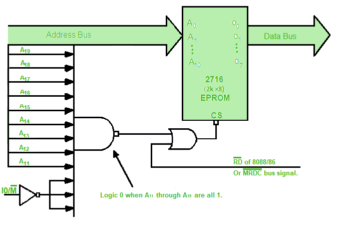
Memory Decoding Circuit
Coincident Decoding:
In the coincident decoding, a decoder with k inputs creates the output with a 2k value. This type of decoder requires 2k AND gates, along with k inputs at each gate. Here, by combining two decoders into a two-dimensional scheme, the total number of gates and inputs per gate could be reduced.
Also, In the bi-dimensional matrix method, one of the decoders is used for row selection and the other for column selection. In this case, two 2k inputs are used instead of one k inputs.
This can be understood with the help of the following diagram:

Two-Dimensional Decoding Structure for a 1k-word memory
Example: Here, instead of using a 10 x 1,024 decoder in the selection method for 1K word of memory, two 5 x 32 decoders can be selected. We need 1,024 AND gates with ten inputs each in a single decoder.
In the case of two decoders, we would need 64 AND gates, each having five inputs. The first five most significant bits are assigned to the input X, and the last five least significant bits are assigned to the input Y. Every word in the memory array is chosen as the result of a coincidence of one X line and one Y input.
As a result, a single word in memory is chosen by the coincidence factor between 1 of 32 rows and 1 or 32 columns, for a total of nearly 1,024 words. The needed word is found at the intersection of a specific row and column. After then, all of the required word bits are read/written.
The Address Multiplexing:
Address multiplexing allows the user to use lesser pins and as a result, a few bus lines on the processor are used. Instead of having separate bus lines for the address and data, the address on the data line can be placed, where, the data is read and saved at the previously read address.
In detail, there are six transistors in SRAM or Static random-access memory. When the transistors are less in size, the high-density memory cells are created.
DRAM or Dynamic random-access memory, also includes a transistor, giving it a larger memory storage capacity than SRAM. SRAM data storage is more expensive than DRAM data storage. DRAM is more energy efficient.
Because the word bit size of DRAM is one, multiple chips are needed. Mainly because of the increased capacity; the decoding of all DRAM bits is performed in a two-dimensional array, and if there is more memory data in a cell, several arrays are needed. Address multiplexing is used by designers to reduce the number of pins in integrated circuits.
Here, the address is separated into two parts for separate groups of times in the two-dimensional array. The addresses for the rows are listed first, followed by the addresses for the columns. The total size is purposely decreased since the same pin set is used for both sides of the memory address.
Example: In multiplexing, a 64K word memory is needed. The two-dimensional array of cells is organized into 256 rows and 256 columns, which then, makes the memory address. This gives a total of 64K words of memory There are two address strobes, a single data input line, a single data output line, a read/write control with an eight-bit address input, and a single data input line. The row addresses strobe abbreviated RAS, which activates the eight-bit memory row register. The column address strobe is truncated because CAS enables the 8-bit column register. The strobe symbol features a bar on top, indicating that the registers are either empty or at the signal’s zero level.
This can be understood with the following diagram:

The Diagram of Address multiplexing
So far, we’ve covered the internal construction and the memory decoding procedure, along with the different aspects of decoding in this article. Finally, we can say that memory decoding is an important yet fundamental aspect of accessing the memory of digital electronic circuitry.
Similar Reads
What is ECC Memory?
Error correction code memory, often known as ECC memory, is a kind of computer data storage that detects and fixes n-bit data corruption in memory using an error correction code (ECC). In this article, we will understand the functionality of ECC Memory, applications of ECC Memory, and more. What is
7 min read
What is a Memory Card?
In this age of digitalization, where most of the information is already converted into digital format a compact chip become basic requirement to store this huge amount information. As result memory card already have become very common in our modern electrical devices, memory card can be considered a
11 min read
What is a Memory Dump ?
A memory dump copies all information from RAM to a storage disk as a memory dump file (*.DMP format). A memory dump generally identifies a problem or error with the operating system or any installed applications on the system. Typically, a memory dump contains information on the final state of progr
4 min read
What is Content-addressable Memory?
Content-Addressable Memory (CAM) is a form of memory that enables faster data retrieval by comparing incoming input to all stored values simultaneously. CAM's high-speed search capabilities is useful for application requiring higher speed such as database maintenance and network switching. CAM is co
5 min read
What is a Bubble Memory ?
Bubble memory is also known as Magnetic Bubble Memory. The inventor Andrew Bobeck invented bubble memory in the 1970s at Bell Labs. Bubble memory comes under the category of non-volatile computer memory. The representation of data is in the form of magnetic bubbles (tiny circular areas) as it uses a
2 min read
What are In-Memory Caches?
In-memory caches are essential tools in modern computing, providing fast access to frequently used data by storing it in memory. This article explores the concept of in-memory caches, their benefits, and their role in enhancing system performance and scalability. Important Topics for In-Memory Cache
12 min read
What is video memory ?
Video memory is a type of memory used to store image data that the computer's GPU (Graphics Processing Unit) needs. Video memory is important for ensuring that graphics work smoothly and efficiently, especially in graphics applications like video games, 3D modeling software, and high-definition vide
6 min read
What is the Caching Mechanism ?
In this article, we will know about the Caching Mechanism, its importance, and basic usage, along with an understanding of its working mechanism, various types of caching & real-time applications. What Is Caching?It is the process of storing and accessing data from memory(i.e. cache memory). The
7 min read
What is One Hot Design?
In the field of computer science and electronics, there are some methods, which are used to represent data in such a way, so that it can be used in machines and computers. These methods are called encoding schemes. One- hot encoding is one of those methods. In this article, we will be discussing one
6 min read
What is Register Memory?
Register memory is a type of computer memory that consists of a small set of storage locations within the central processing unit (CPU) itself. These storage locations, known as registers, are used to store data temporarily during the execution of a program. More and bigger registers allow faster CP
7 min read